
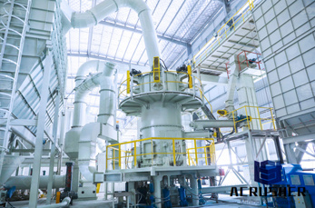
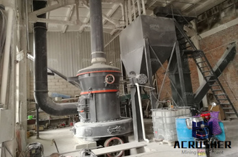
Wafer Back Grinding Process manufacturer Grasping strong production capability, advanced research strength and excellent service, Shanghai Wafer Back Grinding Process supplier create the value and bring values to all of customers.
 WhatsApp)
For 25 years, we have been buying and selling all types of used and refurbished semiconductor equipment from wafer manufacturing through fabrication to backend ...
INTECH | Intech Technologies International (S) Pte. Ltd. We are a team of an experienced energetic entrepreneurs that started INTECH back in year 2008.
Types of Wafer Substrates. A wafer after cleanroom fabrication, ready to be processed into individual parts and packaged.
Thin Silicon Wafers 2um, 5um, 10um, 25um, 50um, 100um all specs to 10mm thick all types and dopants silicon single and double side polsihed and more including, GaAs ...
Wafer Works also provides highquality 4" 8" epitaxial wafers and buried layer epitaxial process services, meeting customer''s power device and CMOS demands and ...
Silicon Wafer Bonding Process. This page contains the basic steps for the successful bonding of silicon wafers. Cleaning Process for Silicon Wafers
Lapping, optical polishing, low stress grinding, diamond machining and honing services. Process details, trade show information, articles.

Wafer Works'' polished silicon wafers consist of 4" 8" low defect, superior flatness silicon wafers, containing dopants such as boron, phosphorus, arsenic, and ...
A short primer explaining how silicon can be packed and delivered to ensure safe transportation with minimum damages.
ICROS TAPE is used to manufacture integrated circuits as a surface protective tape in the silicon wafer backgrinding process.
Semiconductor Manufacturing Equipment USITC Publication 3868 June 2006 OFFICE OF INDUSTRIES International Trade Commission Washington, DC 20436
Syagrus Systems thin wafer backgrinding and silicon wafer thinning services meets company''s demands for extremely thin silicon wafers for use in complex applications.
Engis EHG Horizontal Grinding machines are perfect for backthinning or preparing wafers such as sapphire. Highest level of flatness and surface finish!
Products for DBG Process. BG Tape for DBG Process This is a back grinding tape that fully prevents infiltration of grinding fluid during polishing, as well as the ...
Sapphire Lapping and Polishing Process Single Crystal Sapphire. The use of Single Crystal Sapphire, as a high quality original optomechatronic material in the ...
Silicon carbide (SiC) engineering material properties and typical uses commercially available
Semiconductor Wafer Edge Analysis/4 Stricter requirements in the wafer manufacturing process have made edge measurements important for both 200 mm and .
The 3M ™ Wafer Support System combines proprietary 3M temporary bonding technologies with world class equipment designed specifically to process wafers using
The TAIKO process is a wafer backgrinding method developed by DISCO Corporation. This process method leaves a ring, approximately on the wafer outer ...
Grinding and Polishing GRINDING removes saw marks and levels and cleans the specimen surface. Polishing removes the artifacts of grinding but very little stock.
HSquare is one of the world leaders in cleanroom products for thin Semiconductor wafer handling.
Leadingedge Tape B!_ (B Equipment solution created with semiconductorrelated products ''Adwill.'' Fully and semiautomatic wafer mounters for the dicing process.
Browse GlobalSpec''s Datasheet directory to locate information and specifications for more than 8 million products. The archive is organized by product area; view ...
Leadingedge Tape B!_ (B Equipment solution created with semiconductorrelated products ''Adwill.'' Products that contribute to back grinding processes such as back ...
WhatsApp)